

Heterogeneous integration
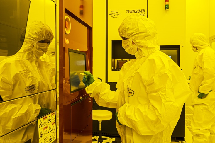
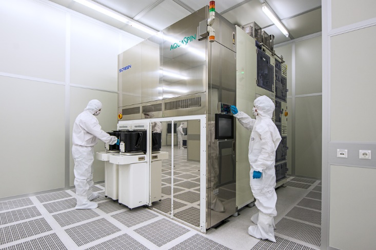
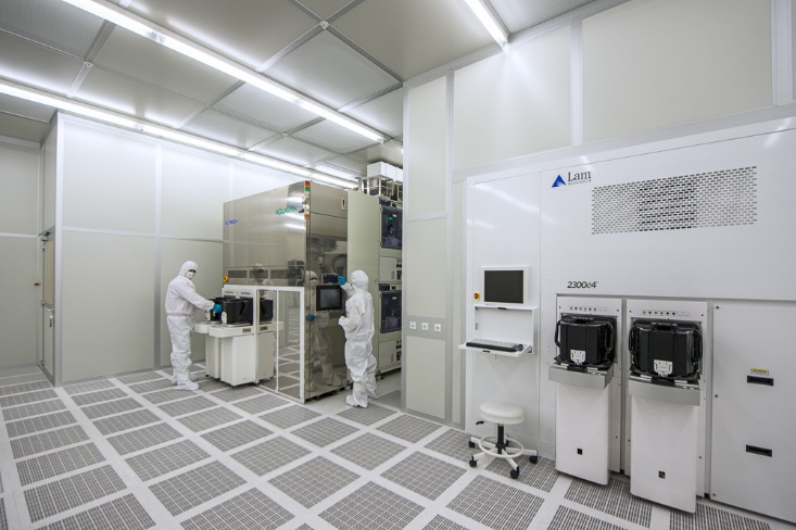
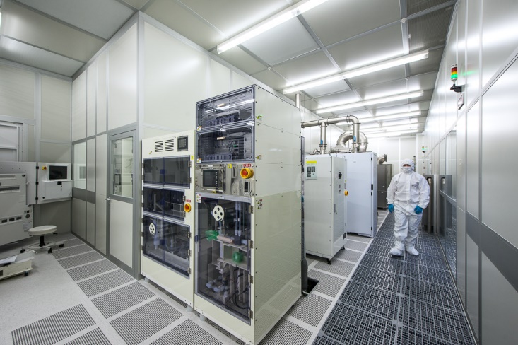
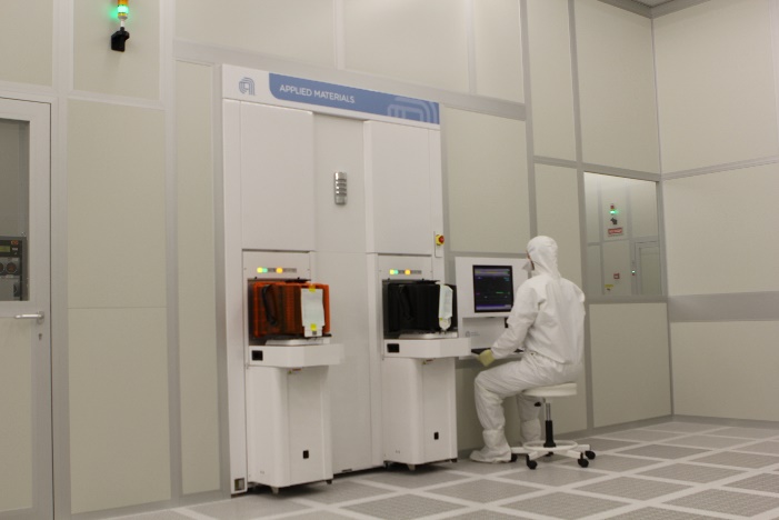
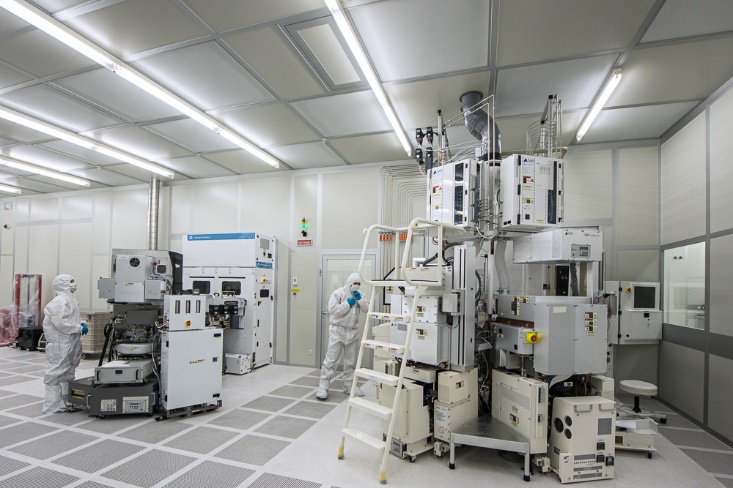
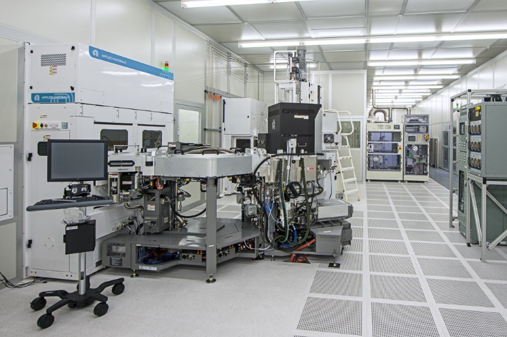
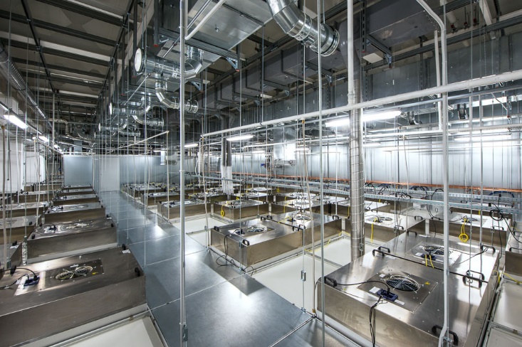
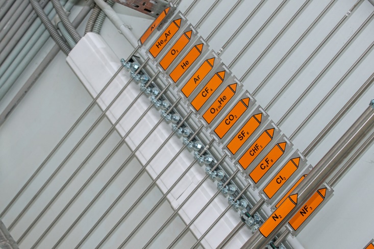
In 2015-2016 INME RAS has developed, completed and put into trial operation to carry out scientific work an experimental line for VLSI metallization on 300 mm plates.
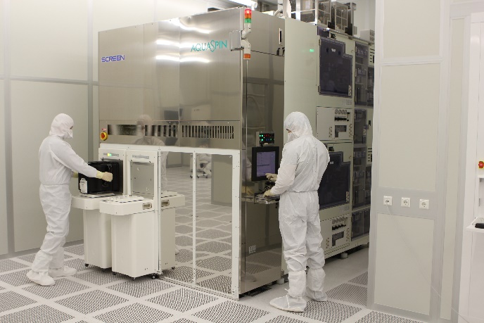
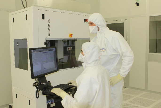
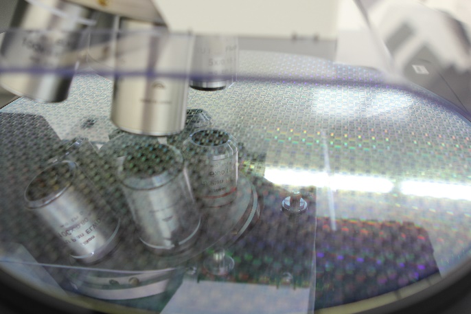
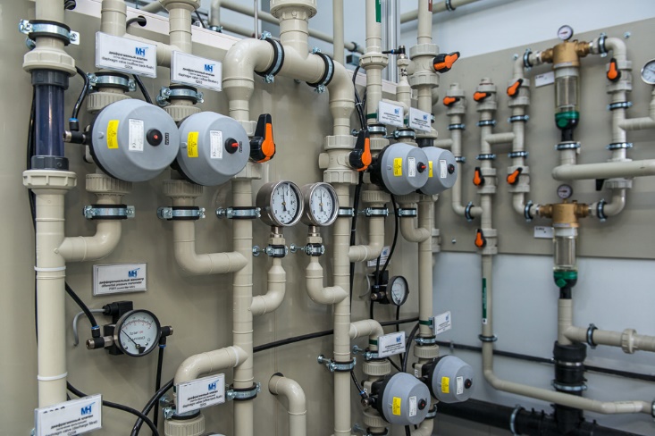
A high-tech engineering infrastructure has been created, instrumental equipment and formulation of precision photolitography processes, metal etching, deposition of passivating dielectric, and opening contact windows have been carried out.
At present, expanding clean rooms, additional technological equipping and setting up processes for sputtering metals, forming interlayer dielectric, and preparing contact areas for forming ball terminals are planned.
Main activity: the formation of a scientific-technical platform for the development and creation of microsystems based on the active interposer.
The basic scientific approach is based on the heterogeneous integration principles — expanding the CMOS process by adding specific steps for integrating active silicon-carbon elements into a crystal body or creating vertically-integrated structures using MEMS crystals or additional memory.
The advantages of the approach are reducing form factor, power consumption and delay time, integrating crystals manufactured using incompatible technologies into a single package.
Application area: internet of things, biomedical systems, industrial and household sensors, telecommunications and the automotive industry.
|

|

|
|
|
|
|
|
|
|
|
|
|
|
|
|
|
|

|
|
|
|

